 隔离型直流电源转换器.docx
- 文档编号:9087247
- 上传时间:2023-02-03
- 格式:DOCX
- 页数:17
- 大小:1,015.52KB
隔离型直流电源转换器.docx
《隔离型直流电源转换器.docx》由会员分享,可在线阅读,更多相关《隔离型直流电源转换器.docx(17页珍藏版)》请在冰豆网上搜索。
隔离型直流电源转换器
隔離型直流電源轉換器
三種本DC-DC轉換器之架構:
buck,boos,buck-boost適用於:
無隔離情況
輸出、輸入電壓倍數相差不大之情況上述情況若無法滿足時,需使用隔離型轉換器常見隔離刑轉換器有:
馳返式(flyback)
順向氏(forward)
推挽式(push-pull)
半波橋式(halfbridge)
全波橋式(fullbridge)
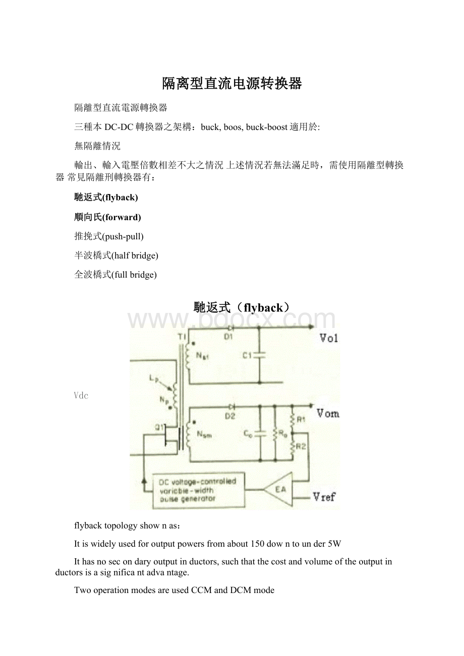
馳返式(flyback)
flybacktopologyshownas:
Itiswidelyusedforoutputpowersfromabout150downtounder5W
Ithasnosecondaryoutputinductors,suchthatthecostandvolumeoftheoutputinductorsisasignificantadvantage.
TwooperationmodesareusedCCMandDCMmode
CCM:
Thecurrentoftheprimaryisalwayslargerthanzero.
DCM:
Thecurrentoftheprimarywillbereducedtozero
Themajortopicistodesignthetransformerselectatransistordiodeandcapacitor
tosatisfythespec.
Np
Ns
TheoperationofDCMmode:
showsasfollows
Step1:
Theturnsratioofprimaryandsecondary
WhenQison,thedroppedvoltageacrosstheprimaryisVL=V,-1.Fromthe
ohms-law:
Vl7-1-Ldi(t)。
So,thei(t)canbedescribedasdt
VI-1
i(t)ti(0)。
Iftheflybackisoperatedatdiscontinuousmode,i(0)=0.So,
i(t)二
VI-1
t.ForfixedcurrentIp,theminimizeinputvoltageVI(min)willinduce
andthecircuitmustberemainedindiscontinuousmode.%*Tr■Ttd=T
二T.Tr=0.8T
12W12
WbLpIpjoulesSo,theinputpower〒盲Lp|p。
Now,the
efficiencyisassumedto80%,wehave
Step4:
Theprimarywireturns
Step5:
Thesecondarywireturns
Step6:
Theprimaryrmscurrentandwiresizemustbecalculated.
T°nandthe
1i|
FromthermsformulaoftheprimaryisIprms:
一Vi2(t)dt=P.
i2(t)dJ3W
<3\TN
Ts'3kT
rmsformulaofthesecondaryisIsrms
Andwiresizeisspecifiedby300~500circularmilesperrmsampere(itjustonlysuggestion
step7:
consideredtheskineffect.
thanskindepth,morewirenumberswillbebetterasinglelargerwiresize.
Step8:
determinethecapacitor
Duringthetransistorontime,theloadcurrentissuppliedbythecapacitor.Theripple
chargeQis:
:
^^IOTon-T°n=C:
V。
So,thevalueofthecapacitoris
RO
C=,whereVistherippleofoutputvoltage.
DCMtoCCMtransition
■Whentheoutputvoltagedecreas(theoutputloadincreasetheoutputresistancedecreasethepeakcurrentofprimarycurrentIpwillbeincreasedfrompointB”toD”.AndtheontimeofthetransistorwillincreasefrompointC”oE”
■Atabovecondition,theofftimeisreducedfromf'”toL”.Thestartcurrentofofftime”isincreasedfromH”toK”.Fromabovefigure,thedeadtimewillbereducedfromTdttozero.ThiscaseistheboundaryofDCM/CCM.
■Iftheloadisstillincreased,theontimewillbeincreased.So,thepeakcurrentofprimaryIPwillbefurthergrowthandofftimewillbedecreased.Whentheontimeofnextcyclestarts,theprimarycurrentIPcan'reducetozero.TheCCMmodeisoperated.
TheoperationofCCMmode:
showsasfollows
Step1:
Theturnsrationofprimaryandsecondary
WhenQisoffstate,thediodeatsecondarysideisturnonandthemirrorvoltagewillreflecttotheprimarysideVP二NpVs.ThevoltageVS二V。
1.Thatis,
Ns
VP二Np(Vo1).So,thetransistorissustainedthevoltagestresVms
Ns
Vms二V|Vp二V|(max)-NP(Vo1)
Ns
Step2:
determinethemaximizeontime
Thecoremustbeguaranteednottosaturated.Thevoltage-timeproductof
ND
6n-time”mustbeequaltooff-time”.Thatis,Vi(minTon二Vo1PToff
Ns
andthecircuitmustberemainedincontinuousmode.ThatisTonToff=T
NP
So,Vi(minTon=!
Vo1-(T-Ton).Itleadsto
Ns
step3:
DeterminetheinductaneeLPofprimary
亠T
lepr
Ton
|csr
toff
Fromabovefig.theoutputpowerPisequaltotheoutputvoltagetimestheaverage
ToffTon
ofthesecondarycurrentpulsesangivenPo=V°Gr〒=V°Icsr(1-〒).Thatis,
(V|(min)T)
dlDCMmodeandCCMmode,thefollowingconditionissatisfiedIcpr
Step4:
Theprimaryrmscurrentandwiresizemustbecalculated.
Andwiresizeisspecifiedby300~500circularmilesperrmsampere
:
」P=300lrmsp。
Fromthermsformulaofsecondary
(亍、T,
V。
1上T
\T丿
step5:
consideredtheskineffect.
o2837
skindepthS二.So,whentheprimaryandsecondarywiremilesarelarger
thanskindepth,morewirenumberswillbebetterasinglelargerwiresizeStep6:
Theprimarywireturns
N一(Wmax一1)hn10*p-Ae
ABo
Vp=V|(max)^NPAeT-108
Vo1
Ion
andNs=Np
spV|(max)-1
Step7:
determinethecapacitor
Duringthetransistorontime,theloadcurrentissuppliedbythecapacitor.Theripple
VO-
chargeQis:
:
Q=lOT°n-T°n=CV。
So,thevalueofthecapacitoris
VOTon
VRo
whereVistherippleofoutputvoltage.
順向氏(forward)
Forwardtopologyshownas:
DV
Itwidelyusedforoutputpowerunder200WwhemmaximumDCinputvoltageisintherangeof60Vto200V
Whentheinputvoltagebelow60Vtheprimaryinputcurrentbecomes
uncomfortablylarge.
Whentheinputvoltageabove200Vthemaximumvoltagestressonthetransistorbecomestolarge.
Comparedtothepush-pulltopology,itismoreeconomicalduetoontransistorbeused.
WhenQ1isturnedon:
CurrentandpowerflowsintothedotendofNp1.AllrectifiersdiodeD2toD4areforward-biasandcurrentandpowersflowstotheloadthroughLCfilter.
V°mr=[(Vdc-1)N^'-Vd2
.Np」
Thevolt-secondproductistheareaA=VdcT°n,duetothefluxchange
WhenQ1off:
ThevoltageacrossNrandNpisVdcandthevoltageattheno-dotendofNpandattheQ1isthen2Vdc.
Forthevolt-secondsareaproductA2isequaltoareaA1.
Inthecommonexpress,theresetvolt-secondshasequaltothesetvolt-seconds.
Therectifierdiodesd2,D3,D4areoffstate,
Thefree-wheelingdiodesD5,D6,D7areonstate.
•Themajortopicistodesignthetransformerselectatransistordiodeandcapacitortosatisfythespec
Step1:
Theturnsrationofprimaryandsecondary
WhenQison,thedroppedvoltageacrosstheprimaryisV_=V|-1.
ThevoltageofthecathodeofD2isthemirroroftheprimaryvoltage
Vomr=(Vi-1-Vd2
INp
TheoutputvoltageistheaverageofVomrthroughthe(L,C)filter.So,
|nordertoensurethecoreinthenon-saturation,theontimeshouldbelesstha5Tfortheminimuminputvoltage.Thatis,
Thedropvoltageofthediodeisassumedas1.V
Step2:
Theprimarywireturnsandsecondaryturns
d二
FromtheFaradayslawV=E.dl.Wehave
dt
5
Vo1
2
andNsNp
Vi(min)-1
Step3:
Thepeakflat-topcurrentofprimary
Thedutycycleoftheprimarypulseis—T/T二0.4。
Theefficiencyofforwardis
..2
JJIZIL
5
thefunctionofL,Cfilteristoaveragethevoltageattherectifiercathodes.Theinductorwillguaranteetheconverterinthecontinuousmod(CCM).Thecapacitorisselectedtoyieldaminimumspecifiedoutputripplevoltage.Consideredtheboundarycondition,thefollowingissatisfied
1
IdcdI.So,
2
dI
Vl=Vrk-Vo=L.WhereVrkisthevoltageoftheanodenodeofdiode
—Ton
Fromthefact「thefunctionofL,Cfilteristoaveragethevoltageatthe
rectifiercathodes」
T-
wehaveVo=Vrk21andT°n=0.4T.Theinductoris
T
*Theripplealmostdeterminedbytheequivalentseriesresistance^ofthecapacitor.Thepeak-to-peakrippleVor=Rdl
ThealuminumelectrolyticcapacitorhasthecharacteristicRC。
=6510"
sv/itchingfrequ&ncy
Zerocurrent
推挽式(push-pull)topology
push-pulltopologyshownas
ItconsistsofatransformerT1,withmultiplesecondaries
Twoequalandadjustable-width180outofphasearesuppliedtodrivetheswitchofQ1,Q2FeedbackloopisclosedaroundVsmandToniscontrolledtoregulateditagainstlineandloadchanges.
TheoutputvoltageVm,Vs1,Vs2are
switchingftequency
AsVdcvaries,thenegative-feedbackloopcorrectsToninsuchadirectionaastokeepVmconstant.
Slavesareregulatedagainstlinebutonlypartiallyagainstload.
Half-bridgetopology
Half-bridgetopologyshownas:
ItsmajoradvantageisthatitsubjectstheofftransistortoonlyVdc.
Thecircuitalwaysyieldroughly320VofrectifiedDcvoltagewhetherinputis120or220Vac
WhenQ1isonandQ2off,thedotendofNpis168Vpositivewithrespecttoitsno-dotendandtheoffstressonQ2isonly336V
WhenQ2isonandQ1off,thedotendofNpis168Vnegativewithrespecttoitsno-dotendandQ1is336Vreversed.
Full-bridgetopology:
Fullbridgetopologyshownas:
ThevoltageimpressedacrosstheprimaryoffullbridgeisVdccomparedto0.5Vdcforthehalf-bridge
ThefullbridgecandelivertwicethepowerofthehalfbridgeatsameconditionDiagonallyoppositetransistors(Q2andQ3orQ4andQ1areturnedonsimultaneouslyduringalternatecycle.
Theoutputvoltagesareshown:


- 配套讲稿:
如PPT文件的首页显示word图标,表示该PPT已包含配套word讲稿。双击word图标可打开word文档。
- 特殊限制:
部分文档作品中含有的国旗、国徽等图片,仅作为作品整体效果示例展示,禁止商用。设计者仅对作品中独创性部分享有著作权。
- 关 键 词:
- 隔离 直流电源 转换器
 冰豆网所有资源均是用户自行上传分享,仅供网友学习交流,未经上传用户书面授权,请勿作他用。
 《城市规划基本知识》深刻复习要点.docx
-
《高电压技术》word版.docx
-
《安全带》gb6095.docx
-
BCP计划应急计划.docx
-
《计算机组成与工作原理》第一章复习题.docx
-
CANON LBP系列激光打印机使用方法指南.docx
-
C语言课程设计火车票系统源代码.docx
-
3热力管道沟槽开挖方法.docx
-
HR岗位职责.docx
-
1 脱硫脱硝cems维护技术规范.docx
-
O2O超市商业项目计划书.docx
-
SCI期刊呼吸胸外.docx
-
18岁生日祝福语短信.docx
-
ITMC物流企业经营沙盘比赛规则.docx
-
XX钢绳成本管理.docx
-
Matlab的第三方工具箱大全强烈推荐.docx
-
安全保卫工作先进个人.docx
-
安全生产工作日记.docx
-
windows 漏洞集合.docx
-
Φ160数控落地镗铣床技术规格.docx
-
安全施工组织设计.docx
-
安全检查和隐患排查治理制度及记录.docx
-
部编版小学二年级语文下册课外阅读专项.docx
-
变电站投运前质量监督检查汇报材料模版.docx
-
版 创新设计 高考总复习 历史 北师大版第一部分 必考内容第十五单元 第38讲.docx
-
本科毕业设计论文.docx
-
北京大学社会心理学串讲笔记1一10章加试题.docx
-
亳州市教坛新星骨干教师学科带头人特级教师年度考核细则知识分享.docx
-
超星尔雅《人生与人心》期末考试满分答案.docx
-
财经法规与会计职业道德案例分析题.docx
-
茶文化会发言稿.docx
-
财务会计核算实习总结.docx
-
数学教学心得体会3篇.docx
-
万科地产设计管理工作标准景观设计供参考.docx
-
生物高考大一轮复习热点题型九基因在染色体的位置判断讲义北师大版精装版.docx
-
集体合同存在的问题.docx
-
英文人生价值的名言警句.docx
-
有机房电梯监督检验自检报告.docx
-
辽宁省营口市中考语文试题图片版含答案.docx
-
三八红旗手事迹材料6篇.docx
-
数字信号处理知识点整理Chapter.docx
-
网络工程合同书完整版.docx
-
实验流行病学研究习题及答案.docx
-
医务人员个人防护用品使用的标准操作规程.docx
-
市地方税务局创建标准化分局工作总结.docx
-
数字电视转模拟电视方案.docx
-
临汾市中考数学猜题卷及答案.docx
-
计算机科学与技术专业 外文翻译 外文文献 英文文献 记录.docx
-
学前班家长会总结反思.docx
-
驾考理论知识学习重点难点易错及技巧科目一.doc
-
高新区新建小学教务计划2013年春.doc
