 TBFNG数据手册.pdf
- 文档编号:3209523
- 上传时间:2022-11-20
- 格式:PDF
- 页数:11
- 大小:576.05KB
TBFNG数据手册.pdf
《TBFNG数据手册.pdf》由会员分享,可在线阅读,更多相关《TBFNG数据手册.pdf(11页珍藏版)》请在冰豆网上搜索。
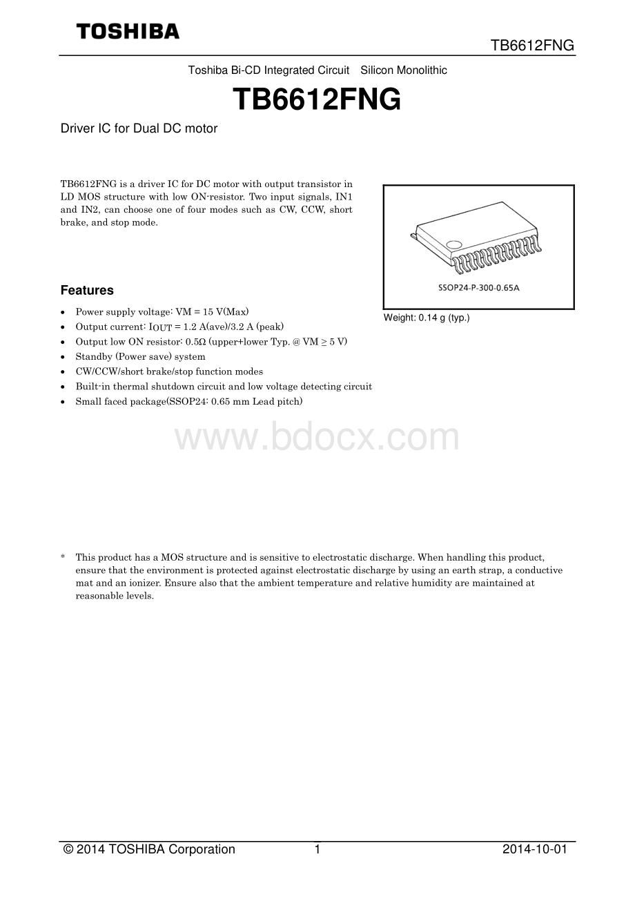
TB6612FNGToshibaBi-CDIntegratedCircuitSiliconMonolithicTB6612FNGDriverICforDualDCmotorTB6612FNGisadriverICforDCmotorwithoutputtransistorinLDMOSstructurewithlowON-resistor.Twoinputsignals,IN1andIN2,canchooseoneoffourmodessuchasCW,CCW,shortbrake,andstopmode.FeaturesPowersupplyvoltage:
VM=15V(Max)Outputcurrent:
IOUT=1.2A(ave)/3.2A(peak)OutputlowONresistor:
0.5(upper+lowerTyp.VM5V)Standby(Powersave)systemCW/CCW/shortbrake/stopfunctionmodesBuilt-inthermalshutdowncircuitandlowvoltagedetectingcircuitSmallfacedpackage(SSOP24:
0.65mmLeadpitch)*ThisproducthasaMOSstructureandissensitivetoelectrostaticdischarge.Whenhandlingthisproduct,ensurethattheenvironmentisprotectedagainstelectrostaticdischargebyusinganearthstrap,aconductivematandanionizer.Ensurealsothattheambienttemperatureandrelativehumidityaremaintainedatreasonablelevels.Weight:
0.14g(typ.)2014TOSHIBACorporation2014-10-011TB6612FNGBlockDiagramPinFunctionsNo.PinNameI/OFunction1AO1OchAoutput12AO13PGND1PowerGND14PGND15AO2OchAoutput26AO27BO2OchBoutput28BO29PGND2PowerGND210PGND211BO1OchBoutput112BO113VM2Motorsupply14VM315PWMBIchBPWMinput/200kpull-downatinternal16BIN2IchBinput2/200kpull-downatinternal17BIN1IchBinput1/200kpull-downatinternal18GNDSmallsignalGND19STBYI“L”=standby/200kpull-downatinternal20VccSmallsignalsupply21AIN1IchAinput1/200kpull-downatinternal22AIN2IchAinput2/200kpull-downatinternal23PWMAIchAPWMinput/200kpull-downatinternal24VM1Motorsupply2014-10-012TB6612FNGAbsoluteMaximumRatings(Ta=25C)OperatingRange(Ta=-20to85C)CharacteristicsSymbolRatingUnitRemarksSupplyvoltageVM15VVCC6InputvoltageVIN-0.2to6VIN1,IN2,STBY,PWMpinsOutputvoltageVOUT15VO1,O2pinsOutputcurrentIOUT1.2APer1chIOUT(peak)2tw=20msContinuouspulse,Duty20%3.2tw=10msSinglepulsePowerdissipationPD0.78WIConly0.8950mm50mmt=1.6mmCu40%inPCBmounting1.3676.2mm114.3mmt=1.6mmCu30%inPCBmountingOperatingtemperatureTopr-20to85CStoragetemperatureTstg-55to150CCharacteristicsSymbolMinTyp.MaxUnitRemarksSupplyvoltageVCC2.735.5VVM2.5513.5VOutputcurrent(H-SW)IOUT1.0AVM4.5V0.44.5VVM2.5VWithoutPWMOperationSwitchingfrequencyfPWM100kHz入力端子;IN1,IN2,PWM,STBYVccGNDInputInternalcircuit200k出力端子;O1,O2VMPGNDO1O2Inputpin:
Outputpin:
O1,O2O1O2VM2014-10-013TB6612FNGH-SWControlFunctionInputOutputIN1IN2PWMSTBYOUT1OUT2ModeHHH/LHLLShortbrakeLHHHLHCCWLHLLShortbrakeHLHHHLCWLHLLShortbrakeLLHHOFF(Highimpedance)StopH/LH/LH/LLOFF(Highimpedance)StandbyH-SWOperatingDescriptionTopreventpenetratingcurrent,deadtimet2andt4isprovidedinswitchingtoeachmodeintheIC.VMVMVMMVMGNDt5MVMGNDt4MGNDMGNDt3MGNDt2t1OUT2OUT1OUT1OUT1OUT1OUT1OUT2OUT2OUT2OUT2GNDVMOUT1Voltagewavet1t2t3t5t42014-10-014TB6612FNGElectricalCharacteristics(unlessotherwisespecified,Ta=25C,Vcc=3V,VM=5V)CharacteristicsSymbolTestConditionMinTyp.MaxUnitSupplycurrentICC(3V)STBY=Vcc=3V,VM=5V1.11.8mAICC(5.5V)STBY=Vcc=5.5V,VM=5V1.52.2ICC(STB)STBY=0V1AIM(STB)1ControlinputvoltageVIHVcc0.7Vcc+0.2VVIL-0.2Vcc0.3ControlinputcurrentIIHVIN=3V51525AIILVIN=0V1StandbyinputvoltageVIH(STB)Vcc0.7Vcc+0.2VVIL(STB)-0.2Vcc0.3StandbyinputcurrentIIH(STB)VIN=3V51525AIIL(STB)VIN=0V1OutputsaturatingvoltageVsat(U+L)1IO=1A,Vcc=VM=5V0.50.7VVsat(U+L)2IO=0.3A,Vcc=VM=5V0.150.21OutputleakagecurrentIL(U)VM=VOUT=15V1AIL(L)VM=15V,VOUT=0V-1RegenerativediodeVFVF(U)IF=1A11.1VVF(L)11.1LowvoltagedetectingvoltageUVLD(Designtargetonly)1.9VRecoveringvoltageUVLC2.2Responsespeedtr(Designtargetonly)24nstf41DeadtimeHtoLPenetrationprotecttime(Designtargetonly)50LtoH230ThermalshutdowncircuitoperatingtemperatureTSD(Designtargetonly)175CThermalshutdownhysteresisTSD202014-10-015TB6612FNGTargetcharacteristicsPD-Ta0.000.501.001.50050100150Ta()(w)IC単体j-a=160/W基板実装時PCB面積50501.6mmCu箔面積40%基板実装時PCB面積76.2114.31.6mmCu箔面積30%IConlyja=160C/WInboardingPCBarea50mm50mm1.6mmCuarea40%InboardingPCBarea76.2mm114.3mm1.6mmCuarea30%PowerdissipationPDPD-TaTa=25C,IConly1chdriving2chdrivingIout-Duty0.00.51.01.52.02.50%20%40%60%80%100%Duty(A)2ch動作時1ch動作時Ta=25,IC単体OutputcurrentIOUTIOUT-DutyDual-channeloperationSingle-channeloperationTa=25C,IConly2014-10-016TB6612FNGTypicalApplicationDiagramNote:
Condensersfornoiseabsorption(C1,C2,C3,andC4)shouldbeconnectedascloseaspossibletotheIC.+4.5V13.5V+C110uFC20.1uFMMCUMCUSTBYAIN1AIN2PWMAH-SWDriverA18TSDVccGND2AO124VM1ControlLogicA20212223193PGND1BIN1BIN2PWMBControlLogicB17161


- 配套讲稿:
如PPT文件的首页显示word图标,表示该PPT已包含配套word讲稿。双击word图标可打开word文档。
- 特殊限制:
部分文档作品中含有的国旗、国徽等图片,仅作为作品整体效果示例展示,禁止商用。设计者仅对作品中独创性部分享有著作权。
- 关 键 词:
- TBFNG 数据 手册
 冰豆网所有资源均是用户自行上传分享,仅供网友学习交流,未经上传用户书面授权,请勿作他用。
 (完整word版)信息论与编码期末考试题----学生复习用.doc
-
(完整)六年级上册几何图形题.docx
-
(完整)储罐防腐施工方案.doc
-
(完整word版)公务员录用体检表.doc
-
(完整)八年级上册几何证明题专项练习.doc
-
(决策管理)投资决策委员会实施细则.doc
-
(完整)四年级上册口算、竖式计算、脱式计算.doc
-
(压轴题)初中物理八年级上册第一章《机械运动》检测(含答案解析)(2).doc
-
(完整)小学三年级心理健康教案.doc
-
(完整)初中文言文翻译技巧.doc
-
(名师整理)语文中考《骆驼祥子》名著导读优秀教案.docx
-
(完整word版)偏旁部首名称大全.doc
-
(人教PEP)五年级英语竞赛试题及答案.doc
-
(完整)山东省普通高中学生综合素质评价信息管理系统操作手册学生用户手册.doc
-
(完整word版)体育课教案模板.doc
-
(住宅楼方案)房屋建筑学课程设计说明书.doc
-
(完整word版)《分数的意义》优秀教学设计(公开课).doc
-
(完整word版)安全生产标准化实施方案.doc
-
(完整)初中生人物形象分析常用词汇.doc
-
(完整版)借用公司资质协议.doc
-
(完整word版)仙剑奇侠传三图文攻略(最详细版).doc
-
(完整word版)历年陕西省专升本英语真题(答案解析超全).doc
-
(完整)四年级四则混合运算训练题100道.doc
-
(完整word版)学校团总支部换届选举方案.doc
-
(完整word版)安全标准化绩效评定计划.doc
-
(完整)分布式光伏发电项目施工组织设计.doc
-
(完整版)埋地塑料管结构环刚度计算.doc
-
(完整版)国家农业产业强镇示范建设实施方案.doc
-
(完整版)八年级数学上几何典型试题及答案.doc
-
(完整版)六年级音乐下册人音版理论知识梳理.doc
-
(完整版)囚徒健身图文教程和计划表(完美打印版).doc
 (完整版)固定资产盘点表.xls
-
小学五年级体育教案全集版.docx
-
开学第一课XX观后感200字.docx
-
苏教版小学数学四年级下册全册说课稿汇编.docx
-
新版教科版小学四年级科学下册全册教案.docx
-
消防组织架构图.xls
-
新版人教版pep小学英语3至6年级知识点归纳.docx
-
完整高层建筑结构设计复习试题含答案推荐文档.docx
-
体育之研究读后感作文800字精选4篇.docx
-
小型榨油机项目可行性研究报告.docx
-
我国云管理平台软件综合发展态势图文分析报告.docx
-
大唐四不两直稿件.docx
-
物业管理市场的管理体制.docx
-
图书馆18年全民阅读活动总结.docx
-
酒店人力资源部年度总结及下年度工作计划.doc
-
无人零售行业分析报告.docx
-
现代农牧业科技示范园可行性研究报告.docx
-
贫困学生资助工作总结.doc
-
新人教版版九年级月考物理试题C卷检测.docx
-
小学语文基础知识文学常识手册最必备.docx
