 基于FPGA进行VGA控制器设置实现显示器条纹显示Word文档下载推荐.docx
- 文档编号:17686385
- 上传时间:2022-12-08
- 格式:DOCX
- 页数:21
- 大小:1.13MB
基于FPGA进行VGA控制器设置实现显示器条纹显示Word文档下载推荐.docx
《基于FPGA进行VGA控制器设置实现显示器条纹显示Word文档下载推荐.docx》由会员分享,可在线阅读,更多相关《基于FPGA进行VGA控制器设置实现显示器条纹显示Word文档下载推荐.docx(21页珍藏版)》请在冰豆网上搜索。
1.像素时钟配置为25Mhz。
2.编写代码时,需要用到的常数参考表一。
3.输出到显示器上的条纹为从上到下依次为RGBRGB(640*80)。
4.本实验使用FPGA板:
Sparant3EXC3S500E(建project时,需要选择板的型号)。
实验方法、步骤:
1、基本设计思想如下图所示:
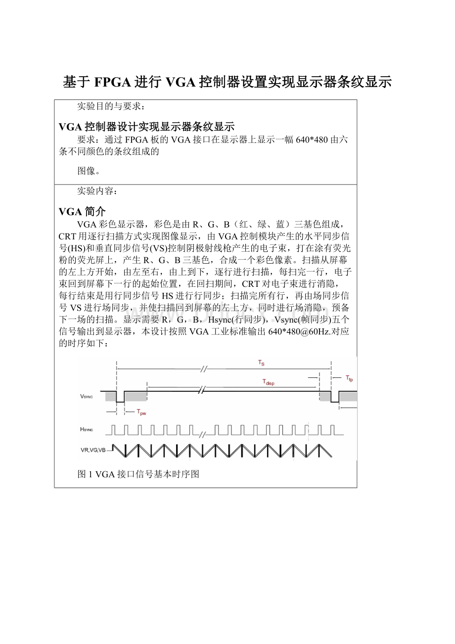
分为这四个模块,产生Hsync(行同步),Vsync(帧同步)以与RGB色彩的输出。
2、具体设计VHDL代码
libraryIEEE;
useIEEE.STD_LOGIC_1164.ALL;
useIEEE.STD_LOGIC_ARITH.ALL;
useIEEE.STD_LOGIC_UNSIGNED.ALL;
entitymainis
port(clk,rst:
instd_logic;
Vsync,Hsync:
outstd_logic;
data:
outstd_logic_vector(7downto0)
);
endmain;
architectureBehavioralofmainis
componentdcnis---------DCM分频模块,输出25M时钟
port(CLKIN_IN:
instd_logic;
RST_IN:
CLKFX_OUT:
outstd_logic;
----输出时钟
CLKIN_IBUFG_OUT:
LOCKED_OUT:
outstd_logic);
endcomponent;
signaldiv_25m,Nrst:
std_logic;
signalVsys_20b:
std_logic_vector(19downto0);
signalHsys_10b:
std_logic_vector(9downto0);
signaldata_Vsend,data_Hsend:
std_logic;
signalScan_16b:
std_logic_vector(15downto0);
signalScan_clc:
signaldata_sel:
std_logic_vector(1downto0);
begin
div:
dcnportmap(clk,Nrst,div_25m,open,open);
---分频模块
Nrst<
=notrst;
process(div_25m,rst)
begin
ifrst='
0'
then
Vsys_20b<
="
00000000000000000000"
;
elsifdiv_25m'
eventanddiv_25m='
1'
=Vsys_20b+1;
ifVsys_20b=416799then
Vsys_20b<
endif;
endif;
endprocess;
process(div_25m,rst,Vsys_20b)
Vsync<
='
data_Vsend<
ifVsys_20b<
8000then
Vsync<
elsifVsys_20b>
=8000andVsys_20b<
9600then
elsifVsys_20b>
=9600andVsys_20b<
32800then--128*255+160=32800
=32800andVsys_20b<
416800then
Hsys_10b<
0000000000"
=Hsys_10b+1;
ifHsys_10b=799then
Hsys_10b<
endif;
process(div_25m,rst,Hsys_10b)
Hsync<
data_Hsend<
ifHsys_10b<
16then
Hsync<
elsifHsys_10b>
=16andHsys_10b<
112then
elsifHsys_10b>
=112andHsys_10b<
160then
=160andHsys_10b<
800then
process(div_25m,rst,data_Vsend)
then--
Scan_16b<
0000000000000000"
Scan_clc<
then---
Scan_clc<
ifdata_Vsend='
then
=Scan_16b+1;
ifScan_16b=63999then
Scan_clc<
process(rst,div_25m,Scan_clc,data_sel,data_Vsend)
data_sel<
00"
ifScan_clc='
=data_sel+1;
endif;
ifdata_sel="
11"
data_sel<
process(rst,div_25m,data_Vsend,data_Hsend)
data<
00000000"
ifdata_Vsend='
anddata_Hsend='
casedata_selis
when"
=>
11000000"
when"
01"
00111000"
10"
00000111"
whenothers=>
endcase;
else
data<
endBehavioral;
UCF管脚定义:
NET"
clk"
LOC="
P183"
NETclkIOSTANDARD=LVCMOS33;
rst"
P142"
#
PULLUP;
IOSTANDARD=LVCMOS33;
data(0)"
P74"
#
data
(1)"
P75"
data
(2)"
P76"
data(3)"
P77"
data(4)"
P78"
data(5)"
P82"
data(6)"
P83"
data(7)"
P89"
Vsync"
P68"
Hsync"
P69"
DCM设置:
综合结果:
综合分析:
仿真波形
实际测试:
实验结论:
本实验设计达到了实验要求,产生了预期效果,通过本实验,进一步了解了如何设计FPGA外部设备的驱动时钟,对计数器的设计有了更深一步的认识。
进一步熟悉了FPGA涉与的过程以与方法
指导教师批阅意见:
成绩评定:
指导教师签字:
年月日
备注:
注:
1、报告内的项目或内容设置,可根据实际情况加以调整和补充。
2、教师批改学生实验报告时间应在学生提交实验报告时间后10日内。


- 配套讲稿:
如PPT文件的首页显示word图标,表示该PPT已包含配套word讲稿。双击word图标可打开word文档。
- 特殊限制:
部分文档作品中含有的国旗、国徽等图片,仅作为作品整体效果示例展示,禁止商用。设计者仅对作品中独创性部分享有著作权。
- 关 键 词:
- 基于 FPGA 进行 VGA 控制器 设置 实现 显示器 条纹 显示
 冰豆网所有资源均是用户自行上传分享,仅供网友学习交流,未经上传用户书面授权,请勿作他用。
 《雷雨》中的蘩漪人物形象分析 1.docx
-
《经济法基础》第三章章节练习与答案解析.docx
-
安徽省合肥市包河区卫生健康系统招聘试题及答案解析.docx
-
《河中石兽》复习过程.docx
-
版二级建造师《公路工程管理与实务》考前检测 附答案.docx
-
保密安全制度监理组5篇修改版.docx
-
北师大版届九年级上学期期末考试英语试题I卷.docx
-
PACE产品及周期优化法系统结构复习课程.docx
-
常规变电站常规设计.docx
-
初三欧姆定律计算题题型整理.docx
-
《测绘管理与法律法规》模拟试题一附答案.docx
-
2测风工岗位练兵技术比武.docx
-
《小学语文不同课型的教学模式参考》1.docx
-
15高考宁夏英语及答案教学内容.docx
-
ABS圆形笔筒课程设计说明书.docx
-
c语言程序填空题.docx
-
茶艺师高级三级教学计划大纲.docx
-
场平土石方工程施工项目组织设计.docx
-
《人力资源管理》期末试题及答案教学内容.docx
-
《河南省高等学校教师实验人员中高级专业技术职务任职资格申报评审条件试行.docx
-
01钢结构制作施工工艺标准文档.docx
-
IIR数字滤波器的设计流程图.docx
-
005纺丝作业指导书.docx
-
1991高考化学试题.docx
-
GMP审核检查表与审核员指南.docx
-
成本会计试题二.docx
-
14001讲师心态调整培训讲座讲义体验版共14页文档.docx
-
cpld矩阵键盘.docx
-
《金融服务营销》.docx
-
NHR100过程校验仪140408.docx
-
Q+ Web 改版设计小结.docx
-
八年级上册古诗词鉴赏含参考答案.docx
-
计算机选择题Word文件下载.docx
-
浪漫港湾桩基施工及水上钢平台施工方案1Word文档下载推荐.docx
-
健康教育知识试题题库及答案Word文档格式.docx
-
2大型危化装置全表面火灾事故消防装备配备及扑救方法分析Word文档格式.docx
-
湖南师大附中学年高二下学期入学考试 语文 扫描版含答案Word文件下载.docx
-
关于服装品牌店销售方面的调研报告Word文档下载推荐.docx
-
故意犯罪形态研究上中共中央党校文档格式.docx
-
顺丰服务标准管理分析Word下载.docx
-
《尼尔斯骑鹅旅行记》读后感15篇Word格式.docx
-
《工程勘察设计收费管理规定》解释文档格式.docx
-
教师专业成长心得体会精选多篇Word下载.docx
-
《将进酒》原文及翻译高中语文基础知识归纳高中docWord文档下载推荐.docx
-
西方行政学说形考三Word下载.docx
-
中考作文技法系列讲座6Word格式文档下载.docx
-
基于双减政策下数学作业有效设计学习心得领会范文5篇Word下载.docx
-
《乡下人家》教学反思文档格式.docx
-
数字图像处理图像校正Word格式文档下载.docx
-
中考科学物理部分题型训练四实验综合题Word文件下载.docx
-
优美句子摘抄大全文档格式.docx
